Industries · Semiconductor
Wafer & Semiconductor Packaging
Plating chemistry for wafer-level packaging, TGV applications and advanced interconnects.
Overview
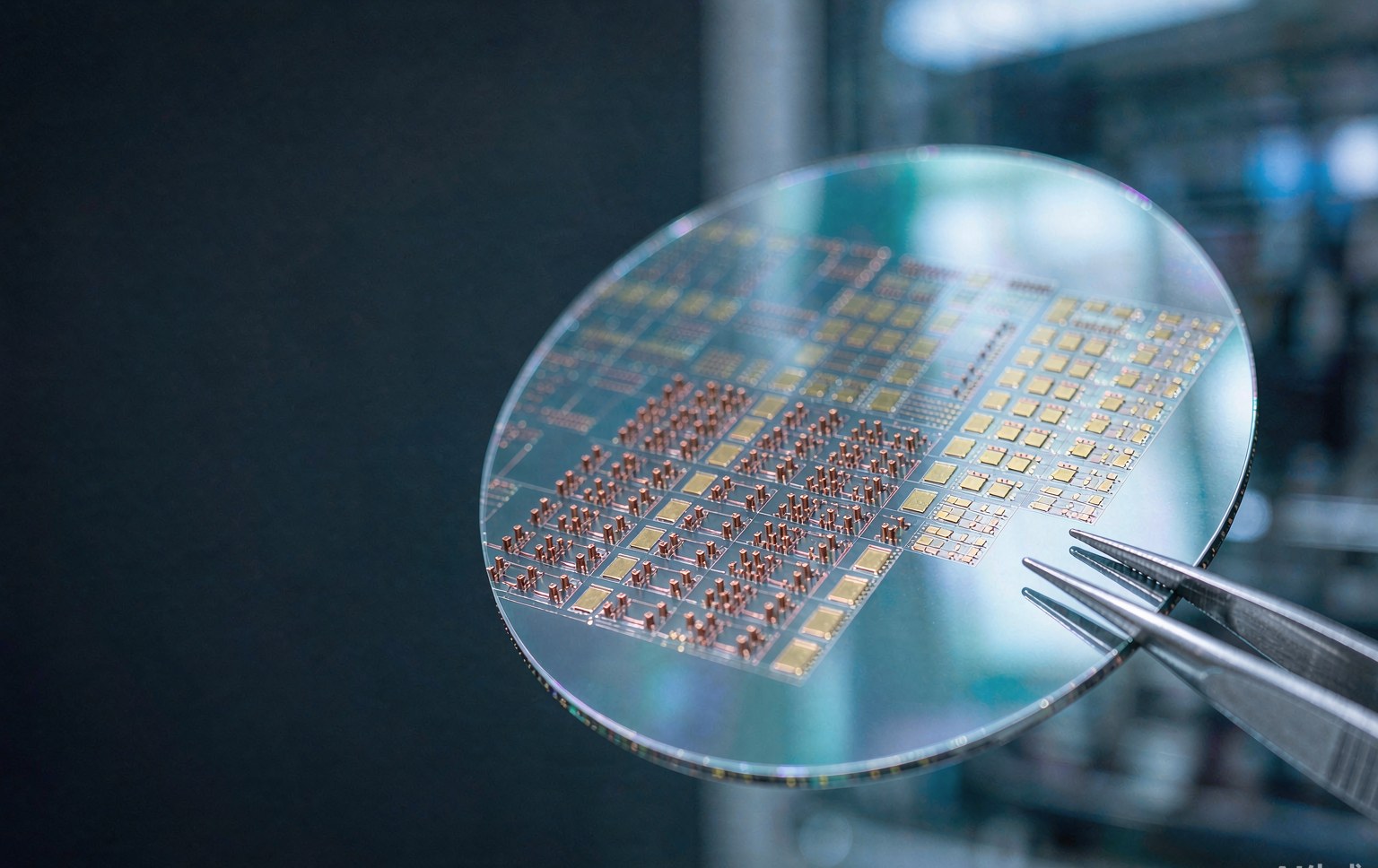
Advanced packaging moves the performance bottleneck into the metallization step. We supply chemistry for UBM, RDL, pillar and TGV filling, engineered for fine features, uniform thickness across the wafer and predictable bath ageing.
- UBM and RDL metallization for wafer-level packaging
- Through-glass via (TGV) and high-aspect-ratio filling
- Gold, copper, nickel and alloy systems for interconnect layers
- Bath analytics and replenishment models for stable thickness distribution
Related Process Families
Chemistry from our portfolio that supports this industry.
Copper Plating
Via filling and RDL copper with tight thickness uniformity across the wafer.
Surface Finishes
ENEPIG and immersion systems for reliable wire-bond and solder interfaces.
Electronic Plating
Gold, nickel and silver processes for interconnect and contact metallization.
Discuss Your Application
Send us your substrate, line type and performance targets — we will recommend the right process and share comparable case data.